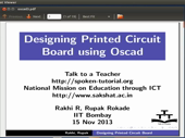
Designing Printed Circuit Board - English
This is a sample video. To access the full content,
please
Login
3219 visits
Outline:
Modify Schematic for PCB design Create netlist for PCB from Schematic Map footprints to components Change layout design rules Choose layers and lay tracks for layout Check for design rules Generate Gerber files


